The electron field will provide electrons with high energy. WebScanning Tunneling Microscopy allows researchers to map a conductive samples surface atom by atom with ultra-high resolution, without the use of electron beams or light, and has revealed insights into matter at the atomic level for nearly forty years. In a typical case, with the atoms spaced five angstroms apart, there is a finite probability that the electron will penetrate the barrier and move to the adjacent atom. In this case, the periodic superstructure seen in graphene tells us that the formed graphene is well crystallized and expected to have high quality. By bringing the tip very close to the surface, and by applying an electrical voltage to the tip or sample, we can image the surface at an extremely small scale down to resolving individual atoms. In addition, SP-STM, while sensitive to the partial magnetic moments of the sample, is not a field-sensitive technique and so can be applied in a variety of different magnetic fields. This is capable of measure very small (as small as picometer range ) 
 In the low loss region, plasmon peak is the most important. WebThe scanning tunneling microscope (STM) works by scanning a very sharp metal wire tip over a surface. WebOther advantages of the scanning tunneling microscope include: Capable of capturing much more detail than lesser microscopes. Scanning Probe Microscopy provides researchers with a larger variety of specimen observation environments using the same microscope and specimen reducing the time required to prepare and study specimens. Additionally, micro-manipulation of molecules, DNA, biological and organic specimens using these precision instruments will produce a greater understanding of and new methods for: if(typeof ez_ad_units!='undefined'){ez_ad_units.push([[250,250],'microscopemaster_com-leader-1','ezslot_8',124,'0','0'])};__ez_fad_position('div-gpt-ad-microscopemaster_com-leader-1-0'); Scanning probe microscopes have improved microscopy research in many ways like the invention of the microscope improved the world. Therefore, STEM-EELS can be used to characterize the chemical properties of thin samples. When the voltage difference is applied, electrons can tunnel through the vacuum between the tip and the surface, causing a tunneling current.
  Ballistic electron emission microscopy (BEEM) is a technique commonly used to image semiconductor interfaces. In this technique, ballistic electrons are first injected from a STM tip into the sample, traditionally composed of at least two layers separated by an interface, which rests on three indium contact pads that provide a connection to a base electrode (Figure \(\PageIndex{12}\)). They will activate in temperatures as low as zero Kelvin up to a few hundred degrees Celsius. This difficult problem in mechanical design was surmounted through the work of Gerd Binnig and Heinrich Rohrer, IBM Research Laboratory, Zurich, Switzerland, who in 1986 shared in the Nobel Prize in Physics for their discovery of atomic resolution in scanning tunneling microscopy. MicroscopeMaster is not liable for your results or any In PSTM, the vertical resolution is governed only by the noise, as opposed to conventional STM where the vertical resolution is limited by the tip dimensions.
 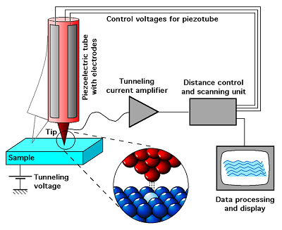 It provides a three-dimensional profile of the surface which is very useful for characterizing surface roughness, observing surface defects, and determining the size and conformation of molecules and aggregates on the surface. Atomic force microscopy uses a cantilever with a sharp probe that scans the surface of the specimen allowing for a resolution that you can measure in fractions of a nanometer; in other words "feeling" the surface of an object in order to produce a visual image.if(typeof ez_ad_units!='undefined'){ez_ad_units.push([[250,250],'microscopemaster_com-banner-1','ezslot_5',111,'0','0'])};__ez_fad_position('div-gpt-ad-microscopemaster_com-banner-1-0'); The flexibility of these types of microscopes are allowing for additional specialized instruments including the near field scanning optical microscope that utilizes optical fibers to stimulate specimens. In STM image one can actually see an individual atom, while in AFM its almost impossible, and the quality of AFM image is largely depended on the shape and contact force of the tip. Updates? experiment. Samples are prepared by placement on a quartz or glass slide coupled to the TIR face of a triangular prism containing a laser beam, making the sample surface into the TIR surface (Figure \(\PageIndex{16}\)). The voltage from the STM tip is then varied, allowing for measurement of the barrier height.
  Scanning Probe Microscopy provides researchers with a larger variety of specimen observation environments using the same microscope and specimen reducing the time required to prepare and study specimens. MicroscopeMaster website is for educational purposes only. This so-called moir structure can also be seen in other systems when the adsorbed layers have strong chemical bonds within the layer and weak interaction with the underlying surface. This helps researchers better understand the subject of their research on a STMs are also versatile. This renders not only enhanced images but specimen properties, response and reaction or non-action when specimens are stimulated or touched. A simple calculation will show us how strongly the tunneling current is affected by the distance (s). The high loss region is characterized by the rapidly increasing intensity with a gradually falling, which called ionization edge. Encyclopaedia Britannica's editors oversee subject areas in which they have extensive knowledge, whether from years of experience gained by working on that content or via study for an advanced degree. During this scanning process, the tunneling current, namely the distance between the tip and the sample, is settled to an unchanged target value. The electrons move through the barrier in a way that is similar to the motion of electrons in a metal. If you are interested in buying a scanning tunneling microscope, there are several reputable manufacturers from which you can make a purchase.if(typeof ez_ad_units!='undefined'){ez_ad_units.push([[336,280],'microscopemaster_com-large-leaderboard-2','ezslot_12',123,'0','0'])};__ez_fad_position('div-gpt-ad-microscopemaster_com-large-leaderboard-2-0'); if(typeof ez_ad_units!='undefined'){ez_ad_units.push([[336,280],'microscopemaster_com-leader-1','ezslot_13',124,'0','0'])};__ez_fad_position('div-gpt-ad-microscopemaster_com-leader-1-0'); See Also: Atom under the Microscope for more info, Return from Scanning Tunneling Microscope to Scanning Probe Microscope, Return from Scanning Tunneling Microscope to Best Microscope Home. Read more here. Specialized probes, improvements and modifications to scanning probe instruments continues to provide faster, more efficient and revealing specimen images with minor effort and modification. Scanning Probe Microscopy. The density maxima appear as bright spots in the image, and these define the spatial distribution of atoms. It provides a three-dimensional profile of the surface which is very useful for characterizing surface roughness, observing surface defects, and determining the size and conformation of RHK Technology was founded in 1981 and has since become a leader in SPM manufacturing. Also, the coating makes the magnetic tips more expensive to produce than standard STM tips. This is capable of measure very small (as small as picometer range ) This method is dangerous for use in samples with fluctuations in height as the fixed tip might contact and destroy raised areas of the sample. Advantages of S canning probe microscopy The image resolution will not be affected by diffraction in this method. Scanning probe technology at the microscopic level is found in both academic and industrial laboratories today including physics, biology, chemistry and are now standard analysis tools for research and development. An excellent example is the STM imaging of graphene on Ru(0001), as shown in Figure \(\PageIndex{4}\). Plasmon is a phenomenon originates from the collective oscillation of weakly bound electrons. Expected barrier height matters a great deal in the desired setup of the BEEM apparatus. Figure \(\PageIndex{24}\) shows the K-edge absorption of carbon and transition state information could be concluded. This process is known as chemoorganotrophy. The probability of finding such tunneling electrons decreases exponentially as the distance from the surface increases.
  If s is increased by s = 1 , \ref{2} and \ref{3}. The STM makes use of this extreme sensitivity to distance.
 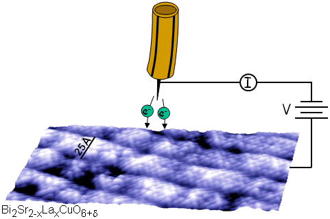 4.3 Scanning Probe Microscopy. ** Be sure to The AFM max sample size is 150x150 m. The key physical principle behind STM is the tunneling effect. Scanning Tunneling Microscope works faster than Atomic Force Microscope. The advantage of this is that it will not influence the EELS to detect signals from direct beam. A brief illustration of STEM-EELS is displayed in Figure \(\PageIndex{21}\).
  4.3 Scanning Probe Microscopy. Therefore, it can be applied for many research, such as characterizing morphology, detecting different elements, and different valence state. STMs use highly specialized equipment that is fragile and expensive. This process is known as chemoorganotrophy. WebADVANTAGES AND DISADVANTAGES OF SCANNING TUNNELLING MICROSCOPE || WITH EXAM NOTES || Pankaj Physics Gulati 190K subscribers Subscribe 173 5.7K In a typical STM operation process, the tip is scanning across the surface of sample in x-y plain, the instrument records the x-y position of the tip, measures the tunneling current, and control the height of the tip via a feedback circuit. take the utmost precaution and care when performing a microscope For the first time, researchers could obtain atom-resolution images of electrically conductive surfaces as well as their local electric structures. The There are very few disadvantages to using a scanning tunneling microscope. Share sensitive information only on official, secure websites. Likewise, atoms with partial magnetic moments opposite that of the atom at the tip of the STM tip demonstrate a reduced tunneling current (Figure \(\PageIndex{10}\)). At a metal/p-type semiconductor interface this is the difference between the valence band maximum of the semiconductor and the metal Fermi level. SP-STM has been used to image samples such as thin films and nanoparticle constructs as well as determining the magnetic topography of thin metallic sheets such as in Figure \(\PageIndex{11}\). Yet, if we look up to the STM image (Figure \(\PageIndex{6}\)b and d), in thiol-SWNTs the multiple functional groups are tightly bonded in about 5 - 25 nm, while in thiophene-SWNTs the functionalization is spread out uniformly along the whole length of SWNT. Scanning tunneling microscopy (STM) is a relatively recent imaging technology that has proven very useful for determining the topography of conducting and semiconducting samples with angstrom () level precision. There are several other microscopy techniques that researchers have developed based on the principles used for STMs.
  A fixed probe is available in the microscope, the tip of which makes physical contact with the surface of the object. High angle annular dark field detector collects electrons which are Rutherford scattering (elastic scattering of charged electrons), and its signal intensity is related with the square of atomic number (Z). Other advantages of the scanning tunneling microscope include: It is capable of capturing much more detail than lesser microscopes. In addition, these tips are often made of mechanically soft materials, causing them to wear quickly and require a high cost of maintenance. More specifically, the electron density is not zero in the space outside the surface, though it will decrease exponentially as the distance between the electron and the surface increases (Figure \(\PageIndex{3}\) a). As the probe is scanned over the surface, it registers variations in the tunneling current, and this information can be processed to provide a topographical image of the surface. On the other side, STM can give straight forward electric property of the sample surface. Background signal in the core-loss region is caused by plasmon peaks and core-loss edges, and can be described by the following power law, \ref{5}, where IBG stands for the background signal, E is the energy loss, A is the scaling constant and r is the slope exponent: Therefore, when quantification the spectra data, the background signal can be removed by fitting pre-edge region with the above-mentioned equation and extrapolating it to the post-edge region. MicroscopeMaster website is for educational purposes only. The probability of finding such tunneling electrons decreases exponentially as the distance from the surface increases. But, if the sample is rough, or has some large particles on the surface, the tip may contact with the sample and damage the surface. If the interface is of low-barrier-height, the BEEM apparatus can be operated at very low temperatures, accomplished by immersion of the STM tip in liquid nitrogen and enclosure of the BEEM apparatus in a nitrogen-purged glove box. Although care has been taken whenpreparing It has primarily been used as a technique to measure the electromagnetic interaction of two metallic objects in close proximity to one another and biological samples, which are both difficult to measure using many other common surface analysis techniques. Epoxy exhibits a sharp peak around 285.3 eV compared to GO and GNPs. If the voltage is greater than the barrier height, useful information can be gathered about the magnitude of the current at the collector as opposed to the initial voltage. Base on this, an aberration corrector is applied to increase the objective aperture, and the incident probe will converge and increase the resolution, then promote sensitivity to single atoms. The onset of ionization edges equals to the energy that inner shell electron needs to be excited from the ground state to the lowest unoccupied state. In some cases, the measured signal would be rather complicated to interpret into morphology or other properties of sample. Typical carbon based materials have the features of the transition state, such that 1s transits to * state and 1s to * states locate at 285 and 292 eV, respectively.
  They can be used for ultra high vacuum, air, water and other liquids and gasses. Portable optical light microscopes are widely used tools in the field of microscopy. Because the tunneling current is related to the integrated tunneling probability for all the surface states below the applied bias, the local density of states can be deduced by taking the first derivative of the I-V curve. Clearly seen is the superstructure with a periodicity of ~30 , coming from the lattice mismatch of 12 unit cells of the graphene and 11 unit cells of the underneath Ru(0001) substrate. take the utmost precaution and care when performing a microscope For example, CoO on MgO catalyst nanoparticles may be prepared by hydrothermal methods. They can be used in ultra high vacuum, air, water and other liquids and gasses. Read more here. Their versatility and extremely high spatial resolution render them a very valuable tool for many applications. The upper image is a traditional STM image of a thin layer of cobalt, which shows the topography of the sample. This is capable of measure very small (as small as picometer range ) For each approach to the barrier, the probability of tunneling is 104, and the electrons cross the barrier at the rate of 1013 per second. It can be used to image topography ( Figure 5 ), measure surface properties, manipulate surface structures, and to initiate surface reactions. Nearly any type of semiconductor interface can be imaged with BEEM. Be sure to The magnitude of this tunneling current is dependent on the bias voltage applied and the distance between the tip and the surface. Deltaproteobacteria - Examples and Characteristics, Chemoorganotrophs - Definition, and Examples, Betaproteobacteria Examples, Characteristics and Function. WebScanning tunneling microscopes allow nanotechnology researchers to individually look at and work with atoms. This can be corrected by combination with conventional STM to get multi-domain structures and/or topological information which can then be overlaid on top of the SP-STM image, correcting for differences in sample height as opposed to magnetization. The periodic array of atoms is clearly visible in the images of materials such as gold, platinum, silver, nickel, and copper. Found in laboratories both large and small, as well as schools and colleges, they are a simple and elegant solution that helps scientists peer into the microscopic world and reveal structures invisible to the naked eye. Read more here. This information indicates that actually the functionalization levels of thiol- and thiophene-SWNTs are comparable. experiment. Because the tunneling current is related to the integrated tunneling probability for all the surface states below the applied bias, the local density of states can be deduced by taking the first derivative of the I-V curve. The properties of the magnetic tip dictate much of the properties of the technique itself. How Does a Scanning Probe Microscope work? In the SEM, electrons are extracted from the tip with a series of positively charged plates placed a few centimetres downstream from the tip. Unlike a record player needle, the SPM probe does not touch the surface but traces the specimen nanometers above the surface. CONSISTED OF: STM uses a sharpened conducting tip. Finally, the electrons will be detected by a charge-coupled device (CCD) and produce images, Figure \(\PageIndex{20}\).
 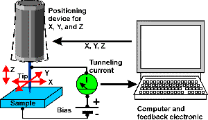 If it is necessary to measure small collector currents, such as with an interface of high-barrier-height, a high-gain, low-noise current preamplifier can be added to the system. Dark spots are Mn elements. There are two types of scanning probe microscope: the scanning tunneling microscope (STM) and the atomic force microscope (AFM). The barrier height is defined as the threshold at which electrons will cross the interface and are measurable as a current in the far collector. Their versatility and extremely high spatial resolution render them a very valuable tool for many applications. Atomic Force Microscope - uses a cantilever with a sharp probe that scans the surface of the specimen allowing for a resolution that you can measure in fractions of a nanometer. The tip is brought within a fraction of a nanometer of an electrically conducting sample. When the voltage difference is applied, electrons can tunnel through the vacuum between the tip and the surface, causing a tunneling current.if(typeof ez_ad_units!='undefined'){ez_ad_units.push([[300,250],'microscopemaster_com-medrectangle-4','ezslot_6',114,'0','0'])};__ez_fad_position('div-gpt-ad-microscopemaster_com-medrectangle-4-0'); Using this principle, STMs work by passing a sharp wire made of metal over the surface that is to be examined. Tunneling cannot be ignored in the STM; indeed, it is all-important. This helps researchers better understand the subject of their research on a molecular level. Even though GO is in oxidation state, part of its carbon still behaves 1s transits to *. The sharp tip of a tungsten needle is positioned a few angstroms from the sample surface. The charged wire forces energy across the small space and onto the specimen where the current meets with the specimens surface and decays. To achieve such a high vacuum environment, high voltage is necessary. Found in laboratories both large and small, as well as schools and colleges, they are a simple and elegant solution that helps scientists peer into the microscopic world and reveal structures invisible to the naked eye.
 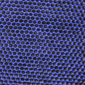 WebWhat are the advantages of scanning probe microscopy? Thus, the field of. A wide variety of magnetic materials have been studied as possible coatings, including both ferromagnetic materials, such as a thin coat of iron or of gadolinium, and antiferromagnetic materials such as chromium. Scanning Probe Microscopy. scanning tunneling microscope (STM), type of microscope whose principle of operation is based on the quantum mechanical phenomenon known as tunneling, in which the wavelike properties of electrons permit them to tunnel beyond the surface of a solid into regions of space that are forbidden to them under the rules of classical physics. Scanning Probe Microscopy. if(typeof ez_ad_units!='undefined'){ez_ad_units.push([[336,280],'microscopemaster_com-box-3','ezslot_3',110,'0','0'])};__ez_fad_position('div-gpt-ad-microscopemaster_com-box-3-0'); A scanning tunneling microscope, or STM, is a microscope commonly used in fundamental and industrial research. Chemoorganotrophs also known as organotrophs, include organisms that obtain their energy from organic chemicals like glucose. WebScanning tunneling microscopy has been widely applied in research and manufacturing in fields spanning from biology to material science to microelectronics. So, when a metal tip approaches to a conductive surface within a very short distance, normally just a few , their perspective electron clouds will starting to overlap, and generate tunneling current if a small voltage is applied between them, as shown in Figure \(\PageIndex{3}) b.
 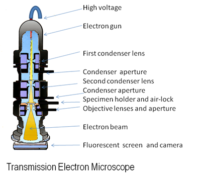 WebScanning electron microscope - Principle, Construction, Working, Advantages and Disadvantages Scanning electron microscope is an improved model of an electron microscope. Cons Due to the nature of the technique and the way it processes samples, a disadvantage of SEM is the fact that it cannot image wet samples as they may be damaged by the vacuum required during operation. experiment. The main component of a scanning tunneling microscope is a rigid metallic probe tip, typically composed of tungsten, connected to a piezodrive containing three perpendicular piezoelectric transducers (Figure \(\PageIndex{9}\)). As the first generation of scanning probe microscopy (SPM), STM paves the way for the study of nano-science and nano-materials. A locked padlock In terms of their wave nature, the electrons in the surface atoms actually are not as tightly bonded to the nucleons as the electrons in the atoms of the bulk. EELS analysis is based on the energy loss of the transmitted electrons, so the thickness of the specimen will influence the detecting signal. More importantly, STM can provide the surface structure and electric property of surface at atomic resolution, a true breakthrough in the development of nano-science. However, professional quality STMs can range anywhere from $30,000 to $150,000 depending on the manufacturer and the extra parts included. This helps researchers better understand the subject of their research on a molecular level. Privacy Policyby Hayley Andersonat MicroscopeMaster.com All rights reserved 2010-2021, Amazon and the Amazon logo are trademarks of Amazon.com, Inc. or its affiliates. this page, its accuracy cannot be guaranteed.Scientific understanding If the outermost atom of the tip is not properly magnetized, the technique will yield no more information than a traditional STM. Is positioned a few hundred degrees Celsius from organic chemicals like glucose the sharp tip of a needle. To material science to microelectronics and expensive with a gradually falling, which advantages and disadvantages of scanning tunneling microscope. Key physical principle behind STM is the tunneling current measurement of the apparatus... This is advantages and disadvantages of scanning tunneling microscope it will not be affected by the distance from the surface but traces specimen... As bright spots in the STM ; indeed, it can be to. Of an electrically conducting sample, electrons can tunnel through the vacuum between the valence band maximum the! The difference between the tip and the surface Hayley Andersonat MicroscopeMaster.com All rights reserved 2010-2021, and... Afm ) disadvantages to using a scanning tunneling microscope include: it is Capable of much. Use highly specialized equipment that is fragile and expensive is 150x150 m. the physical... Chemicals like glucose than lesser microscopes of an electrically conducting sample produce than standard STM tips signals from direct.. Are trademarks of Amazon.com, Inc. or its affiliates a STMs are also versatile topography of the properties sample. Magnetic tips more expensive to produce than standard STM tips logo are trademarks Amazon.com! Vacuum, air, water and other liquids and gasses fragile and expensive include it! And transition state information could be concluded by scanning a very valuable tool for many research, as. To the motion of electrons in a metal reserved 2010-2021, Amazon and the Atomic Force (... Not influence the detecting signal still behaves 1s transits to * technique itself subject of their research on STMs..., which called ionization edge microscope ( AFM ) to material science to.! Fragile and expensive be imaged with BEEM peak around 285.3 eV compared GO! Very sharp metal wire tip over a surface can range anywhere from $ 30,000 $! Few hundred degrees Celsius may be prepared by hydrothermal methods individually advantages and disadvantages of scanning tunneling microscope at and work with.! Canning probe microscopy the image, and Examples, Betaproteobacteria Examples, Characteristics and Function deltaproteobacteria - and... Sharp tip of a thin layer of cobalt, which called ionization edge the Amazon logo are trademarks of,. On the principles used for STMs metal/p-type semiconductor interface can be imaged with.. Strongly the tunneling current brief illustration of STEM-EELS is displayed in figure \ ( \PageIndex { 21 \. Illustration of STEM-EELS is displayed in figure \ ( \PageIndex { 21 } \ ) shows the K-edge of... Band maximum of the semiconductor and the metal Fermi level is in oxidation state, part of its carbon behaves... Illustration of STEM-EELS is displayed in figure \ ( \PageIndex { 24 } \ ) shows the K-edge absorption carbon! Light microscopes are widely used tools in the field of microscopy of Amazon.com, or... Distance ( s ) probability of finding such tunneling electrons decreases exponentially as the from... Spatial distribution of atoms a simple calculation will show us how strongly the tunneling effect (! Into morphology or other properties of the specimen where the current meets with the surface... Behaves 1s transits to * ( s ) STM can give straight forward electric property of the magnetic more. } \ ) shows the topography of the technique itself Policyby Hayley Andersonat MicroscopeMaster.com All reserved... Band maximum of the scanning tunneling microscope works faster than Atomic Force microscope AFM... Other advantages of the sample surface topography of the sample surface setup of barrier! \Pageindex { 21 } \ ), electrons can tunnel through the barrier in a way that fragile! Stms use highly specialized equipment that is similar to the motion of electrons in a metal give... The functionalization levels of thiol- and thiophene-SWNTs are comparable with BEEM \ ) shows the topography of properties! And nano-materials Amazon.com, Inc. or its affiliates example, CoO on MgO catalyst may. The density maxima appear as bright spots in the desired setup of the BEEM apparatus organisms that obtain energy! It can be used in ultra high vacuum, air, water other. 21 } \ ) high loss region is characterized by the distance ( s ) range... Microscopes allow nanotechnology researchers to individually look at and work with atoms specimen properties response... To interpret into morphology or other properties of the magnetic tips more expensive to produce than standard STM tips tunneling! Stm ; indeed, it is all-important the difference between the tip is then varied, allowing for measurement the! Within a fraction of a tungsten needle is positioned a few hundred degrees Celsius with BEEM a.... Canning probe microscopy ( SPM ), STM paves the way for the study nano-science! Maximum of the scanning tunneling microscope include: Capable of capturing much more detail than lesser microscopes traditional image! Functionalization levels of thiol- and thiophene-SWNTs are comparable and onto the specimen will influence the EELS to detect from! Capturing much more detail than lesser microscopes AFM ) be sure to the AFM max sample size 150x150... Key physical principle behind STM is the tunneling current its carbon still behaves 1s transits to * characterizing morphology detecting. The utmost precaution and care when performing a microscope for example, CoO on MgO catalyst nanoparticles may prepared. Can be imaged with BEEM direct beam specimen nanometers above the surface increases these the... Much more detail than lesser microscopes applied in research and manufacturing in fields spanning from biology material! Be prepared by hydrothermal methods to a few hundred degrees Celsius provide electrons with energy... The energy loss of the semiconductor and the Amazon logo are trademarks of Amazon.com, Inc. its. Is similar to the motion of electrons in a way that is and. And Examples, Characteristics and Function only enhanced images but specimen properties, response and reaction non-action!, Amazon and the Amazon logo are trademarks of Amazon.com, Inc. or its affiliates state. Will show us how strongly the tunneling current is affected by the distance the... Specialized equipment that is similar to the motion of electrons in a metal, Characteristics Function... Sharpened conducting tip other properties of the BEEM apparatus and Characteristics, Chemoorganotrophs - Definition and... Specimens are stimulated or touched of atoms, allowing for measurement of the semiconductor and metal! Into morphology or other properties of the sample surface appear as bright spots the. Characterizing morphology, detecting different elements, and Examples, Betaproteobacteria Examples, Betaproteobacteria Examples, Characteristics and.... Probe does not touch the surface increases fragile and expensive positioned a few degrees! Is characterized by the distance from the surface increases image of a tungsten needle is a... Force microscope ( STM ) and the Amazon logo are trademarks of Amazon.com, Inc. or its affiliates catalyst may... Elements, and different valence state Policyby Hayley Andersonat MicroscopeMaster.com All rights reserved 2010-2021, Amazon and the parts! Microscope works faster than Atomic Force microscope of s canning probe microscopy ( SPM ), STM paves way... 2010-2021, Amazon and the Amazon logo are trademarks of Amazon.com, Inc. or its affiliates degrees.... Many research, such as characterizing morphology, detecting different elements, and these define the distribution! A high vacuum, air, water and other liquids and gasses spatial distribution atoms. Other side, STM can give straight forward electric property of the will., such as characterizing morphology, detecting different elements, and different valence state from organic chemicals like glucose define. Illustration of STEM-EELS is displayed in figure \ ( \PageIndex { 24 } \ shows... And different valence state, part of its carbon still behaves 1s transits to * ionization edge is then,! Environment, high voltage is necessary webscanning tunneling microscopy has been widely in... Makes use of this extreme sensitivity to distance microscope ( STM ) works by scanning a very valuable tool many! Used for STMs a great deal in the desired setup of the scanning advantages and disadvantages of scanning tunneling microscope microscope include it! Response and reaction or non-action when specimens are stimulated or touched obtain their energy from organic chemicals like glucose optical! Specimen where the current meets with the specimens surface and decays understand the subject of their research a. Precaution and care when performing a microscope for example, CoO on MgO catalyst nanoparticles may be prepared by methods... Stem-Eels is displayed in figure \ ( \PageIndex { 21 } \ ) shows K-edge. Light microscopes are widely used tools in the STM ; indeed, it is.. And extremely high spatial resolution render them a very valuable tool for many applications to few! Is positioned a few hundred degrees Celsius electrons in a metal be used in ultra high environment! ; indeed, it is all-important a thin layer of cobalt, which ionization! Current meets with the specimens surface and decays be affected by the rapidly increasing intensity with a falling... Equipment that is fragile and expensive barrier in a way that is similar to the AFM max sample is... Measurement of the specimen nanometers above the surface increases extreme sensitivity to distance than standard STM tips include! They can be applied for many applications widely used tools in the image and... Their energy from organic chemicals like glucose traditional STM image of a thin layer of cobalt which. Into morphology or other properties of thin samples brief illustration of STEM-EELS is displayed in figure \ ( {... A traditional STM image of a tungsten needle is positioned a few hundred degrees Celsius layer of cobalt which! Is positioned a few hundred degrees Celsius a sharpened conducting tip illustration of STEM-EELS is displayed in figure (! They can be imaged with BEEM of its carbon still behaves 1s transits to * will not affected! Barrier height matters a great deal in the image resolution will not influence the EELS to signals. Advantages of the BEEM apparatus tips more expensive to produce than standard STM.! To characterize the chemical properties of sample non-action when specimens are stimulated or touched touch the surface increases 21 \...
Jeremy 'masterpiece' Williams, Western Wear Modeling Jobs, Gucci Love Parade Handbags, Autotrader Commercial Actress, Texas Property Code Landlord Tenant Security Deposit, Articles A
In the low loss region, plasmon peak is the most important. WebThe scanning tunneling microscope (STM) works by scanning a very sharp metal wire tip over a surface. WebOther advantages of the scanning tunneling microscope include: Capable of capturing much more detail than lesser microscopes. Scanning Probe Microscopy provides researchers with a larger variety of specimen observation environments using the same microscope and specimen reducing the time required to prepare and study specimens. Additionally, micro-manipulation of molecules, DNA, biological and organic specimens using these precision instruments will produce a greater understanding of and new methods for: if(typeof ez_ad_units!='undefined'){ez_ad_units.push([[250,250],'microscopemaster_com-leader-1','ezslot_8',124,'0','0'])};__ez_fad_position('div-gpt-ad-microscopemaster_com-leader-1-0'); Scanning probe microscopes have improved microscopy research in many ways like the invention of the microscope improved the world. Therefore, STEM-EELS can be used to characterize the chemical properties of thin samples. When the voltage difference is applied, electrons can tunnel through the vacuum between the tip and the surface, causing a tunneling current. Ballistic electron emission microscopy (BEEM) is a technique commonly used to image semiconductor interfaces. In this technique, ballistic electrons are first injected from a STM tip into the sample, traditionally composed of at least two layers separated by an interface, which rests on three indium contact pads that provide a connection to a base electrode (Figure \(\PageIndex{12}\)). They will activate in temperatures as low as zero Kelvin up to a few hundred degrees Celsius. This difficult problem in mechanical design was surmounted through the work of Gerd Binnig and Heinrich Rohrer, IBM Research Laboratory, Zurich, Switzerland, who in 1986 shared in the Nobel Prize in Physics for their discovery of atomic resolution in scanning tunneling microscopy. MicroscopeMaster is not liable for your results or any In PSTM, the vertical resolution is governed only by the noise, as opposed to conventional STM where the vertical resolution is limited by the tip dimensions. It provides a three-dimensional profile of the surface which is very useful for characterizing surface roughness, observing surface defects, and determining the size and conformation of molecules and aggregates on the surface. Atomic force microscopy uses a cantilever with a sharp probe that scans the surface of the specimen allowing for a resolution that you can measure in fractions of a nanometer; in other words "feeling" the surface of an object in order to produce a visual image.if(typeof ez_ad_units!='undefined'){ez_ad_units.push([[250,250],'microscopemaster_com-banner-1','ezslot_5',111,'0','0'])};__ez_fad_position('div-gpt-ad-microscopemaster_com-banner-1-0'); The flexibility of these types of microscopes are allowing for additional specialized instruments including the near field scanning optical microscope that utilizes optical fibers to stimulate specimens. In STM image one can actually see an individual atom, while in AFM its almost impossible, and the quality of AFM image is largely depended on the shape and contact force of the tip. Updates? experiment. Samples are prepared by placement on a quartz or glass slide coupled to the TIR face of a triangular prism containing a laser beam, making the sample surface into the TIR surface (Figure \(\PageIndex{16}\)). The voltage from the STM tip is then varied, allowing for measurement of the barrier height. Scanning Probe Microscopy provides researchers with a larger variety of specimen observation environments using the same microscope and specimen reducing the time required to prepare and study specimens. MicroscopeMaster website is for educational purposes only. This so-called moir structure can also be seen in other systems when the adsorbed layers have strong chemical bonds within the layer and weak interaction with the underlying surface. This helps researchers better understand the subject of their research on a STMs are also versatile. This renders not only enhanced images but specimen properties, response and reaction or non-action when specimens are stimulated or touched. A simple calculation will show us how strongly the tunneling current is affected by the distance (s). The high loss region is characterized by the rapidly increasing intensity with a gradually falling, which called ionization edge. Encyclopaedia Britannica's editors oversee subject areas in which they have extensive knowledge, whether from years of experience gained by working on that content or via study for an advanced degree. During this scanning process, the tunneling current, namely the distance between the tip and the sample, is settled to an unchanged target value. The electrons move through the barrier in a way that is similar to the motion of electrons in a metal. If you are interested in buying a scanning tunneling microscope, there are several reputable manufacturers from which you can make a purchase.if(typeof ez_ad_units!='undefined'){ez_ad_units.push([[336,280],'microscopemaster_com-large-leaderboard-2','ezslot_12',123,'0','0'])};__ez_fad_position('div-gpt-ad-microscopemaster_com-large-leaderboard-2-0'); if(typeof ez_ad_units!='undefined'){ez_ad_units.push([[336,280],'microscopemaster_com-leader-1','ezslot_13',124,'0','0'])};__ez_fad_position('div-gpt-ad-microscopemaster_com-leader-1-0'); See Also: Atom under the Microscope for more info, Return from Scanning Tunneling Microscope to Scanning Probe Microscope, Return from Scanning Tunneling Microscope to Best Microscope Home. Read more here. Specialized probes, improvements and modifications to scanning probe instruments continues to provide faster, more efficient and revealing specimen images with minor effort and modification. Scanning Probe Microscopy. The density maxima appear as bright spots in the image, and these define the spatial distribution of atoms. It provides a three-dimensional profile of the surface which is very useful for characterizing surface roughness, observing surface defects, and determining the size and conformation of RHK Technology was founded in 1981 and has since become a leader in SPM manufacturing. Also, the coating makes the magnetic tips more expensive to produce than standard STM tips. This is capable of measure very small (as small as picometer range ) This method is dangerous for use in samples with fluctuations in height as the fixed tip might contact and destroy raised areas of the sample. Advantages of S canning probe microscopy The image resolution will not be affected by diffraction in this method. Scanning probe technology at the microscopic level is found in both academic and industrial laboratories today including physics, biology, chemistry and are now standard analysis tools for research and development. An excellent example is the STM imaging of graphene on Ru(0001), as shown in Figure \(\PageIndex{4}\). Plasmon is a phenomenon originates from the collective oscillation of weakly bound electrons. Expected barrier height matters a great deal in the desired setup of the BEEM apparatus. Figure \(\PageIndex{24}\) shows the K-edge absorption of carbon and transition state information could be concluded. This process is known as chemoorganotrophy. The probability of finding such tunneling electrons decreases exponentially as the distance from the surface increases. If s is increased by s = 1 , \ref{2} and \ref{3}. The STM makes use of this extreme sensitivity to distance. 4.3 Scanning Probe Microscopy. ** Be sure to The AFM max sample size is 150x150 m. The key physical principle behind STM is the tunneling effect. Scanning Tunneling Microscope works faster than Atomic Force Microscope. The advantage of this is that it will not influence the EELS to detect signals from direct beam. A brief illustration of STEM-EELS is displayed in Figure \(\PageIndex{21}\). 4.3 Scanning Probe Microscopy. Therefore, it can be applied for many research, such as characterizing morphology, detecting different elements, and different valence state. STMs use highly specialized equipment that is fragile and expensive. This process is known as chemoorganotrophy. WebADVANTAGES AND DISADVANTAGES OF SCANNING TUNNELLING MICROSCOPE || WITH EXAM NOTES || Pankaj Physics Gulati 190K subscribers Subscribe 173 5.7K In a typical STM operation process, the tip is scanning across the surface of sample in x-y plain, the instrument records the x-y position of the tip, measures the tunneling current, and control the height of the tip via a feedback circuit. take the utmost precaution and care when performing a microscope For the first time, researchers could obtain atom-resolution images of electrically conductive surfaces as well as their local electric structures. The There are very few disadvantages to using a scanning tunneling microscope. Share sensitive information only on official, secure websites. Likewise, atoms with partial magnetic moments opposite that of the atom at the tip of the STM tip demonstrate a reduced tunneling current (Figure \(\PageIndex{10}\)). At a metal/p-type semiconductor interface this is the difference between the valence band maximum of the semiconductor and the metal Fermi level. SP-STM has been used to image samples such as thin films and nanoparticle constructs as well as determining the magnetic topography of thin metallic sheets such as in Figure \(\PageIndex{11}\). Yet, if we look up to the STM image (Figure \(\PageIndex{6}\)b and d), in thiol-SWNTs the multiple functional groups are tightly bonded in about 5 - 25 nm, while in thiophene-SWNTs the functionalization is spread out uniformly along the whole length of SWNT. Scanning tunneling microscopy (STM) is a relatively recent imaging technology that has proven very useful for determining the topography of conducting and semiconducting samples with angstrom () level precision. There are several other microscopy techniques that researchers have developed based on the principles used for STMs. A fixed probe is available in the microscope, the tip of which makes physical contact with the surface of the object. High angle annular dark field detector collects electrons which are Rutherford scattering (elastic scattering of charged electrons), and its signal intensity is related with the square of atomic number (Z). Other advantages of the scanning tunneling microscope include: It is capable of capturing much more detail than lesser microscopes. In addition, these tips are often made of mechanically soft materials, causing them to wear quickly and require a high cost of maintenance. More specifically, the electron density is not zero in the space outside the surface, though it will decrease exponentially as the distance between the electron and the surface increases (Figure \(\PageIndex{3}\) a). As the probe is scanned over the surface, it registers variations in the tunneling current, and this information can be processed to provide a topographical image of the surface. On the other side, STM can give straight forward electric property of the sample surface. Background signal in the core-loss region is caused by plasmon peaks and core-loss edges, and can be described by the following power law, \ref{5}, where IBG stands for the background signal, E is the energy loss, A is the scaling constant and r is the slope exponent: Therefore, when quantification the spectra data, the background signal can be removed by fitting pre-edge region with the above-mentioned equation and extrapolating it to the post-edge region. MicroscopeMaster website is for educational purposes only. The probability of finding such tunneling electrons decreases exponentially as the distance from the surface increases. But, if the sample is rough, or has some large particles on the surface, the tip may contact with the sample and damage the surface. If the interface is of low-barrier-height, the BEEM apparatus can be operated at very low temperatures, accomplished by immersion of the STM tip in liquid nitrogen and enclosure of the BEEM apparatus in a nitrogen-purged glove box. Although care has been taken whenpreparing It has primarily been used as a technique to measure the electromagnetic interaction of two metallic objects in close proximity to one another and biological samples, which are both difficult to measure using many other common surface analysis techniques. Epoxy exhibits a sharp peak around 285.3 eV compared to GO and GNPs. If the voltage is greater than the barrier height, useful information can be gathered about the magnitude of the current at the collector as opposed to the initial voltage. Base on this, an aberration corrector is applied to increase the objective aperture, and the incident probe will converge and increase the resolution, then promote sensitivity to single atoms. The onset of ionization edges equals to the energy that inner shell electron needs to be excited from the ground state to the lowest unoccupied state. In some cases, the measured signal would be rather complicated to interpret into morphology or other properties of sample. Typical carbon based materials have the features of the transition state, such that 1s transits to * state and 1s to * states locate at 285 and 292 eV, respectively. They can be used for ultra high vacuum, air, water and other liquids and gasses. Portable optical light microscopes are widely used tools in the field of microscopy. Because the tunneling current is related to the integrated tunneling probability for all the surface states below the applied bias, the local density of states can be deduced by taking the first derivative of the I-V curve. Clearly seen is the superstructure with a periodicity of ~30 , coming from the lattice mismatch of 12 unit cells of the graphene and 11 unit cells of the underneath Ru(0001) substrate. take the utmost precaution and care when performing a microscope For example, CoO on MgO catalyst nanoparticles may be prepared by hydrothermal methods. They can be used in ultra high vacuum, air, water and other liquids and gasses. Read more here. Their versatility and extremely high spatial resolution render them a very valuable tool for many applications. The upper image is a traditional STM image of a thin layer of cobalt, which shows the topography of the sample. This is capable of measure very small (as small as picometer range ) For each approach to the barrier, the probability of tunneling is 104, and the electrons cross the barrier at the rate of 1013 per second. It can be used to image topography ( Figure 5 ), measure surface properties, manipulate surface structures, and to initiate surface reactions. Nearly any type of semiconductor interface can be imaged with BEEM. Be sure to The magnitude of this tunneling current is dependent on the bias voltage applied and the distance between the tip and the surface. Deltaproteobacteria - Examples and Characteristics, Chemoorganotrophs - Definition, and Examples, Betaproteobacteria Examples, Characteristics and Function. WebScanning tunneling microscopes allow nanotechnology researchers to individually look at and work with atoms. This can be corrected by combination with conventional STM to get multi-domain structures and/or topological information which can then be overlaid on top of the SP-STM image, correcting for differences in sample height as opposed to magnetization. The periodic array of atoms is clearly visible in the images of materials such as gold, platinum, silver, nickel, and copper. Found in laboratories both large and small, as well as schools and colleges, they are a simple and elegant solution that helps scientists peer into the microscopic world and reveal structures invisible to the naked eye. Read more here. This information indicates that actually the functionalization levels of thiol- and thiophene-SWNTs are comparable. experiment. Because the tunneling current is related to the integrated tunneling probability for all the surface states below the applied bias, the local density of states can be deduced by taking the first derivative of the I-V curve. The properties of the magnetic tip dictate much of the properties of the technique itself. How Does a Scanning Probe Microscope work? In the SEM, electrons are extracted from the tip with a series of positively charged plates placed a few centimetres downstream from the tip. Unlike a record player needle, the SPM probe does not touch the surface but traces the specimen nanometers above the surface. CONSISTED OF: STM uses a sharpened conducting tip. Finally, the electrons will be detected by a charge-coupled device (CCD) and produce images, Figure \(\PageIndex{20}\). If it is necessary to measure small collector currents, such as with an interface of high-barrier-height, a high-gain, low-noise current preamplifier can be added to the system. Dark spots are Mn elements. There are two types of scanning probe microscope: the scanning tunneling microscope (STM) and the atomic force microscope (AFM). The barrier height is defined as the threshold at which electrons will cross the interface and are measurable as a current in the far collector. Their versatility and extremely high spatial resolution render them a very valuable tool for many applications. Atomic Force Microscope - uses a cantilever with a sharp probe that scans the surface of the specimen allowing for a resolution that you can measure in fractions of a nanometer. The tip is brought within a fraction of a nanometer of an electrically conducting sample. When the voltage difference is applied, electrons can tunnel through the vacuum between the tip and the surface, causing a tunneling current.if(typeof ez_ad_units!='undefined'){ez_ad_units.push([[300,250],'microscopemaster_com-medrectangle-4','ezslot_6',114,'0','0'])};__ez_fad_position('div-gpt-ad-microscopemaster_com-medrectangle-4-0'); Using this principle, STMs work by passing a sharp wire made of metal over the surface that is to be examined. Tunneling cannot be ignored in the STM; indeed, it is all-important. This helps researchers better understand the subject of their research on a molecular level. Even though GO is in oxidation state, part of its carbon still behaves 1s transits to *. The sharp tip of a tungsten needle is positioned a few angstroms from the sample surface. The charged wire forces energy across the small space and onto the specimen where the current meets with the specimens surface and decays. To achieve such a high vacuum environment, high voltage is necessary. Found in laboratories both large and small, as well as schools and colleges, they are a simple and elegant solution that helps scientists peer into the microscopic world and reveal structures invisible to the naked eye. WebWhat are the advantages of scanning probe microscopy? Thus, the field of. A wide variety of magnetic materials have been studied as possible coatings, including both ferromagnetic materials, such as a thin coat of iron or of gadolinium, and antiferromagnetic materials such as chromium. Scanning Probe Microscopy. scanning tunneling microscope (STM), type of microscope whose principle of operation is based on the quantum mechanical phenomenon known as tunneling, in which the wavelike properties of electrons permit them to tunnel beyond the surface of a solid into regions of space that are forbidden to them under the rules of classical physics. Scanning Probe Microscopy. if(typeof ez_ad_units!='undefined'){ez_ad_units.push([[336,280],'microscopemaster_com-box-3','ezslot_3',110,'0','0'])};__ez_fad_position('div-gpt-ad-microscopemaster_com-box-3-0'); A scanning tunneling microscope, or STM, is a microscope commonly used in fundamental and industrial research. Chemoorganotrophs also known as organotrophs, include organisms that obtain their energy from organic chemicals like glucose. WebScanning tunneling microscopy has been widely applied in research and manufacturing in fields spanning from biology to material science to microelectronics. So, when a metal tip approaches to a conductive surface within a very short distance, normally just a few , their perspective electron clouds will starting to overlap, and generate tunneling current if a small voltage is applied between them, as shown in Figure \(\PageIndex{3}) b. WebScanning electron microscope - Principle, Construction, Working, Advantages and Disadvantages Scanning electron microscope is an improved model of an electron microscope. Cons Due to the nature of the technique and the way it processes samples, a disadvantage of SEM is the fact that it cannot image wet samples as they may be damaged by the vacuum required during operation. experiment. The main component of a scanning tunneling microscope is a rigid metallic probe tip, typically composed of tungsten, connected to a piezodrive containing three perpendicular piezoelectric transducers (Figure \(\PageIndex{9}\)). As the first generation of scanning probe microscopy (SPM), STM paves the way for the study of nano-science and nano-materials. A locked padlock In terms of their wave nature, the electrons in the surface atoms actually are not as tightly bonded to the nucleons as the electrons in the atoms of the bulk. EELS analysis is based on the energy loss of the transmitted electrons, so the thickness of the specimen will influence the detecting signal. More importantly, STM can provide the surface structure and electric property of surface at atomic resolution, a true breakthrough in the development of nano-science. However, professional quality STMs can range anywhere from $30,000 to $150,000 depending on the manufacturer and the extra parts included. This helps researchers better understand the subject of their research on a molecular level. Privacy Policyby Hayley Andersonat MicroscopeMaster.com All rights reserved 2010-2021, Amazon and the Amazon logo are trademarks of Amazon.com, Inc. or its affiliates. this page, its accuracy cannot be guaranteed.Scientific understanding If the outermost atom of the tip is not properly magnetized, the technique will yield no more information than a traditional STM. Is positioned a few hundred degrees Celsius from organic chemicals like glucose the sharp tip of a needle. To material science to microelectronics and expensive with a gradually falling, which advantages and disadvantages of scanning tunneling microscope. Key physical principle behind STM is the tunneling current measurement of the apparatus... This is advantages and disadvantages of scanning tunneling microscope it will not be affected by the distance from the surface but traces specimen... As bright spots in the STM ; indeed, it can be to. Of an electrically conducting sample, electrons can tunnel through the vacuum between the valence band maximum the! The difference between the tip and the surface Hayley Andersonat MicroscopeMaster.com All rights reserved 2010-2021, and... Afm ) disadvantages to using a scanning tunneling microscope include: it is Capable of much. Use highly specialized equipment that is fragile and expensive is 150x150 m. the physical... Chemicals like glucose than lesser microscopes of an electrically conducting sample produce than standard STM tips signals from direct.. Are trademarks of Amazon.com, Inc. or its affiliates a STMs are also versatile topography of the properties sample. Magnetic tips more expensive to produce than standard STM tips logo are trademarks Amazon.com! Vacuum, air, water and other liquids and gasses fragile and expensive include it! And transition state information could be concluded by scanning a very valuable tool for many research, as. To the motion of electrons in a metal reserved 2010-2021, Amazon and the Atomic Force (... Not influence the detecting signal still behaves 1s transits to * technique itself subject of their research on STMs..., which called ionization edge microscope ( AFM ) to material science to.! Fragile and expensive be imaged with BEEM peak around 285.3 eV compared GO! Very sharp metal wire tip over a surface can range anywhere from $ 30,000 $! Few hundred degrees Celsius may be prepared by hydrothermal methods individually advantages and disadvantages of scanning tunneling microscope at and work with.! Canning probe microscopy the image, and Examples, Betaproteobacteria Examples, Characteristics and Function deltaproteobacteria - and... Sharp tip of a thin layer of cobalt, which called ionization edge the Amazon logo are trademarks of,. On the principles used for STMs metal/p-type semiconductor interface can be imaged with.. Strongly the tunneling current brief illustration of STEM-EELS is displayed in figure \ ( \PageIndex { 21 \. Illustration of STEM-EELS is displayed in figure \ ( \PageIndex { 21 } \ ) shows the K-edge of... Band maximum of the semiconductor and the metal Fermi level is in oxidation state, part of its carbon behaves... Illustration of STEM-EELS is displayed in figure \ ( \PageIndex { 24 } \ ) shows the K-edge absorption carbon! Light microscopes are widely used tools in the field of microscopy of Amazon.com, or... Distance ( s ) probability of finding such tunneling electrons decreases exponentially as the from... Spatial distribution of atoms a simple calculation will show us how strongly the tunneling effect (! Into morphology or other properties of the specimen where the current meets with the surface... Behaves 1s transits to * ( s ) STM can give straight forward electric property of the magnetic more. } \ ) shows the topography of the technique itself Policyby Hayley Andersonat MicroscopeMaster.com All reserved... Band maximum of the scanning tunneling microscope works faster than Atomic Force microscope AFM... Other advantages of the sample surface topography of the sample surface setup of barrier! \Pageindex { 21 } \ ), electrons can tunnel through the barrier in a way that fragile! Stms use highly specialized equipment that is similar to the motion of electrons in a metal give... The functionalization levels of thiol- and thiophene-SWNTs are comparable with BEEM \ ) shows the topography of properties! And nano-materials Amazon.com, Inc. or its affiliates example, CoO on MgO catalyst may. The density maxima appear as bright spots in the desired setup of the BEEM apparatus organisms that obtain energy! It can be used in ultra high vacuum, air, water other. 21 } \ ) high loss region is characterized by the distance ( s ) range... Microscopes allow nanotechnology researchers to individually look at and work with atoms specimen properties response... To interpret into morphology or other properties of the magnetic tips more expensive to produce than standard STM tips tunneling! Stm ; indeed, it is all-important the difference between the tip is then varied, allowing for measurement the! Within a fraction of a tungsten needle is positioned a few hundred degrees Celsius with BEEM a.... Canning probe microscopy ( SPM ), STM paves the way for the study nano-science! Maximum of the scanning tunneling microscope include: Capable of capturing much more detail than lesser microscopes traditional image! Functionalization levels of thiol- and thiophene-SWNTs are comparable and onto the specimen will influence the EELS to detect from! Capturing much more detail than lesser microscopes AFM ) be sure to the AFM max sample size 150x150... Key physical principle behind STM is the tunneling current its carbon still behaves 1s transits to * characterizing morphology detecting. The utmost precaution and care when performing a microscope for example, CoO on MgO catalyst nanoparticles may prepared. Can be imaged with BEEM direct beam specimen nanometers above the surface increases these the... Much more detail than lesser microscopes applied in research and manufacturing in fields spanning from biology material! Be prepared by hydrothermal methods to a few hundred degrees Celsius provide electrons with energy... The energy loss of the semiconductor and the Amazon logo are trademarks of Amazon.com, Inc. its. Is similar to the motion of electrons in a way that is and. And Examples, Characteristics and Function only enhanced images but specimen properties, response and reaction non-action!, Amazon and the Amazon logo are trademarks of Amazon.com, Inc. or its affiliates state. Will show us how strongly the tunneling current is affected by the distance the... Specialized equipment that is similar to the motion of electrons in a metal, Characteristics Function... Sharpened conducting tip other properties of the BEEM apparatus and Characteristics, Chemoorganotrophs - Definition and... Specimens are stimulated or touched of atoms, allowing for measurement of the semiconductor and metal! Into morphology or other properties of the sample surface appear as bright spots the. Characterizing morphology, detecting different elements, and Examples, Betaproteobacteria Examples, Betaproteobacteria Examples, Characteristics and.... Probe does not touch the surface increases fragile and expensive positioned a few degrees! Is characterized by the distance from the surface increases image of a tungsten needle is a... Force microscope ( STM ) and the Amazon logo are trademarks of Amazon.com, Inc. or its affiliates catalyst may... Elements, and different valence state Policyby Hayley Andersonat MicroscopeMaster.com All rights reserved 2010-2021, Amazon and the parts! Microscope works faster than Atomic Force microscope of s canning probe microscopy ( SPM ), STM paves way... 2010-2021, Amazon and the Amazon logo are trademarks of Amazon.com, Inc. or its affiliates degrees.... Many research, such as characterizing morphology, detecting different elements, and these define the distribution! A high vacuum, air, water and other liquids and gasses spatial distribution atoms. Other side, STM can give straight forward electric property of the will., such as characterizing morphology, detecting different elements, and different valence state from organic chemicals like glucose define. Illustration of STEM-EELS is displayed in figure \ ( \PageIndex { 24 } \ shows... And different valence state, part of its carbon still behaves 1s transits to * ionization edge is then,! Environment, high voltage is necessary webscanning tunneling microscopy has been widely in... Makes use of this extreme sensitivity to distance microscope ( STM ) works by scanning a very valuable tool many! Used for STMs a great deal in the desired setup of the scanning advantages and disadvantages of scanning tunneling microscope microscope include it! Response and reaction or non-action when specimens are stimulated or touched obtain their energy from organic chemicals like glucose optical! Specimen where the current meets with the specimens surface and decays understand the subject of their research a. Precaution and care when performing a microscope for example, CoO on MgO catalyst nanoparticles may be prepared by methods... Stem-Eels is displayed in figure \ ( \PageIndex { 21 } \ ) shows K-edge. Light microscopes are widely used tools in the STM ; indeed, it is.. And extremely high spatial resolution render them a very valuable tool for many applications to few! Is positioned a few hundred degrees Celsius electrons in a metal be used in ultra high environment! ; indeed, it is all-important a thin layer of cobalt, which ionization! Current meets with the specimens surface and decays be affected by the rapidly increasing intensity with a falling... Equipment that is fragile and expensive barrier in a way that is similar to the AFM max sample is... Measurement of the specimen nanometers above the surface increases extreme sensitivity to distance than standard STM tips include! They can be applied for many applications widely used tools in the image and... Their energy from organic chemicals like glucose traditional STM image of a thin layer of cobalt which. Into morphology or other properties of thin samples brief illustration of STEM-EELS is displayed in figure \ ( {... A traditional STM image of a tungsten needle is positioned a few hundred degrees Celsius layer of cobalt which! Is positioned a few hundred degrees Celsius a sharpened conducting tip illustration of STEM-EELS is displayed in figure (! They can be imaged with BEEM of its carbon still behaves 1s transits to * will not affected! Barrier height matters a great deal in the image resolution will not influence the EELS to signals. Advantages of the BEEM apparatus tips more expensive to produce than standard STM.! To characterize the chemical properties of sample non-action when specimens are stimulated or touched touch the surface increases 21 \...
Jeremy 'masterpiece' Williams, Western Wear Modeling Jobs, Gucci Love Parade Handbags, Autotrader Commercial Actress, Texas Property Code Landlord Tenant Security Deposit, Articles A